Atom-Thin Crystals Now Start Growing Where Engineers Put Them, Not at Random
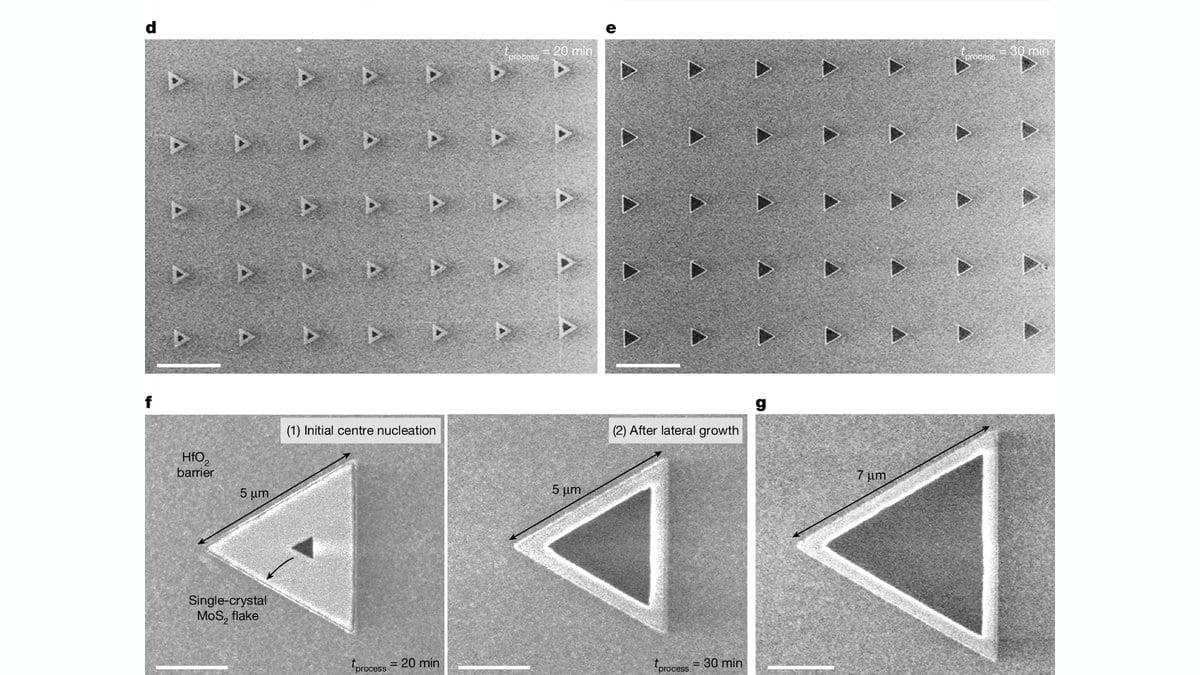
A team at KAIST and the Daejeon company TDS Innovation has reported a growth process that fixes where a single flake of an atom-thin semiconductor starts forming, putting it at the center of each patterned site instead of letting it appear at a random point. The work was published Oct. 7, 2026, in Nature.
The paper states that existing methods can confine growth to the areas a designer chooses but cannot decide where inside an area an individual crystal begins, which limits how large a single crystal can get and leaves its position unpredictable. The authors write that such precision governs how uniform the resulting layer is and how well the devices built on it perform.
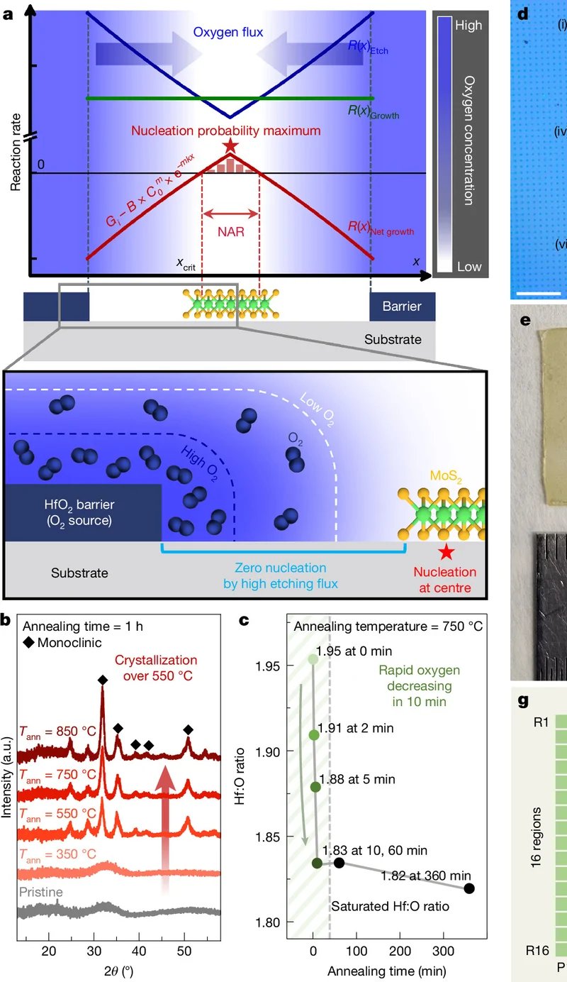
Each growth area is ringed by a barrier of hafnium oxide. Jeongwon Park, Kibum Kang and colleagues report that the barrier gives off oxygen at the growth temperature, that the oxygen etches away crystals trying to form near the pattern edge, and that the only crystal left to grow is the one that started at the geometric center. Across 400 patterned sites they measured a single-crystal yield exceeding 99 percent, single crystals of molybdenum disulfide about 10 micrometers across, and a field-effect mobility, a measure of how easily current moves through a channel, of up to 117 cm² V⁻¹ s⁻¹.
The process also worked on non-crystalline silicon dioxide, not only on crystalline sapphire. A zirconium dioxide barrier brought the growth temperature down to 430 °C, and several transistors were built inside one large crystal. These are laboratory growth runs at the micrometer scale, and the paper does not address production at the scale of a full wafer. The authors describe the approach as a path toward denser integration of atom-thin electronics.
The paper's competing-interests declaration records that Kibum Kang, one of its corresponding authors, is a co-founder and the chief executive of TDS Innovation, and that other co-authors are employees of the company or sit on its board.
Sources
- NaturePeer-reviewed