A Power Chip on Ordinary Silicon Blocks Almost 4,000 Volts
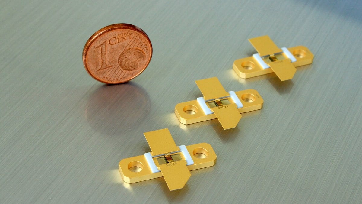
A group at EPFL reports gallium nitride diodes, grown on silicon wafers, that block more than 3.9 kilovolts before breaking down while their on-resistance, measured per unit of chip area, stays as low as 4.7 milliohm square centimeters. Luca Mazzone, Elison Matioli and colleagues published the measurements Aug. 28 in Nature Electronics.
Those two numbers normally pull against each other. A power device holds off voltage across a drift region, and lengthening that region raises both the voltage it blocks and the resistance it adds. A superjunction breaks the trade-off by putting equal amounts of positive and negative charge in the region, so it stays electrically neutral when the device is off. The field then spreads out evenly instead of spiking at the contact edges, where the paper says breakdown usually starts.
Silicon superjunctions are built by doping, which gallium nitride resists: magnesium, the standard p-type dopant, activates poorly, and the authors write that mature implantation and regrowth techniques do not exist. Their devices instead use the material's own spontaneous and piezoelectric polarization to induce a sheet of mobile electrons and a matching sheet of mobile holes, with no intentional doping. An electrical contact to the hole sheet lets both drain during switching.
The diode that exceeded 3.9 kV had a superjunction 25 micrometers long, the paper states. The group also reports transistors that sustain more than 3.4 kV without field plates (the metal layers usually added to smooth the electric field) and dynamic on-resistance degradation under 15 percent up to 3 kV. Breakdown was repeatable and temperature-stable, the authors report, and, in their words, "avalanche-like."
Commercial gallium nitride devices rated at 650 volts typically use multiple field plates, according to the paper. Lateral polarization superjunctions in gallium nitride have been reported before, but the authors write that most relied on doped p-type layers, and that the resulting voltage gains could stem from a field-plate effect rather than true charge balancing.
Gallium nitride can be grown on silicon wafers eight inches across and larger, the paper notes, while other wide-bandgap semiconductors are restricted to smaller wafers.
Sources
- www.nature.comPeer-reviewed