A Laser Bakes a Crystal Onto a Chip Without Cooking the Chip

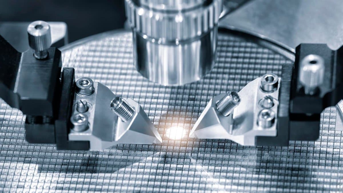
Light does not like to travel in only one direction. Send a beam down a channel etched into silicon and some of it comes back, off a bend, off a joint, off the point where one material meets another. For most of the chip that does not matter. For the laser at the far end it matters a great deal.
A laser fed its own reflected light turns noisy and unsteady, which is why almost every serious optical system contains a one-way gate called an optical isolator. Bench-top isolators have been sold for decades. Building one onto the same piece of silicon as the laser has stayed out of reach, and the obstacle is not optics. It is heat.
An isolator needs a magnetic crystal, usually a garnet, that twists light as it passes through. The direction of the twist is set by a magnet rather than by the light, so a beam going forward and a beam coming back are not treated the same way, and only one of them gets out the far side. The garnet has to be crystalline to do this. Crystallizing it the usual way means putting the whole chip in a furnace, and the heat degrades the silicon waveguides and the metal electrodes around it.
A team at Kyocera and Tohoku University's Research Institute of Electrical Communication has found a way to leave the furnace out, and published it in IEEE Access on Sept. 2, 2026. Tomoya Sugita of Kyocera is the paper's first author, Taichi Goto of Tohoku University its senior author. They deposited the garnet by ion beam sputtering, a vacuum coating method, straight into trenches a few micrometers wide inside a silicon interferometer. No underlayer was laid down first to help the film grow. Then they crystallized it with a 915-nanometer laser beam, in vacuum, aimed at the garnet and nothing else. The surrounding circuit and electrodes came through intact, the team reports. Electron microscopy shows the crystallized garnet sitting on the silicon, with a thin boundary region where the two meet.
The device works as a gate. In the direction it is meant to block, it cuts light by 13.6 decibels at a wavelength of 1540 nanometers. Beside that figure the paper puts a second one: an insertion loss of 20.4 decibels, which is what the gate costs the light it is supposed to let through. Put in percentages, the device stops roughly 95 percent of the light coming back, and about 99 percent of the light going forward. It loses more in the direction it is meant to pass than it blocks in the direction it is meant to stop.
The film's own propagation loss is 9.5 decibels, less than half the total, so the light is not simply being swallowed by the garnet on its way through.
The Sept. 11 announcement from Kyocera and Tohoku University does not give the insertion loss or propagation loss. It focuses on the isolation, the share of reflected light the device removes, and the manufacturing process. It says the conventional furnace route needs 600 °C or more, puts the laser-treated patch at roughly 700 micrometers on a side, and sets the work against data-center hardware that puts light sources next to the switching chips. The release also says the researchers aim to reduce optical loss, but gives no wavelength.
This is not the group's first isolator built onto silicon. On June 12, 2026 much the same team reported one in ACS Applied Optical Materials that blocks more backward light than this one does. That device's garnet was crystallized in a furnace, on a slow temperature ramp, which solved the problem of film quality and left the problem of heat exactly where it was. The laser-annealed version is the trade-off run the other way: a weaker isolator, and a far easier thing to put onto a circuit that is already finished.
This is similar to what was described in this article. However, the focus here is more on the method than on the part: that thermally sensitive silicon devices and thin films needing high-temperature processing can be built together by a technique compatible with mass production. A gate that throws away almost all of the light it is meant to pass is not going into a data center. A way to crystallize a high-temperature material on one patch of a finished wafer, leaving the rest of it cold, may be worth more than the gate is.
Sources
- Peer-reviewedIEEE Access
- doi.org
- eurekalert.org